You can't buy Nvidia B200 or Rubin clusters if Washington has your name on an export blacklist. For Chinese AI giants, that isn't a hypothetical problem; it's the daily reality shaping their engineering decisions. When the US restricted advanced GPU shipments, the immediate reaction across mainland tech hubs was a desperate scramble to hoard legacy silicon and squeeze performance out of sub-optimal architectures.
But brute-forcing performance out of throttled hardware hits a physical wall very quickly.
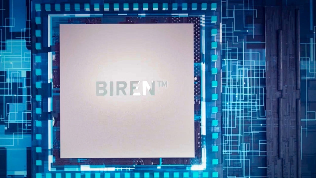
Shanghai-based chip designer Biren Technology isn't trying to out-build Nvidia at its own game anymore. They're changing the game's physical medium. By teaming up with photonics specialist Lightelligence (also known as Xizhi Technology), telecom powerhouse ZTE, and Shanghai INESA, Biren has commercialized what they call the LightLeap SuperNode. Instead of relying solely on copper wires and traditional electronic switches to link GPUs together, this system passes data using photons.
It turns out that changing the plumbing inside the data center might be exactly how China builds a parallel AI ecosystem that doesn't care about semiconductor sanctions.
The Scaling Wall Copper Cannot Scale Over
Building massive AI models like DeepSeek V3 or GPT-4 isn't just a matter of having fast chips. The real bottleneck is communication. When thousands of GPUs work together on a single massive training workload, they spend an enormous amount of time talking to each other. They share weight updates, synchronize parameters, and pass data back and forth constantly.
In a standard data center, this data travels through copper traces on printed circuit boards and thick copper cables between server racks. Copper has serious limitations:
- Resistance and Heat: As you push more data through copper at higher speeds, resistance creates massive heat loads.
- Distance Degradation: High-frequency electronic signals degrade after just a few meters, requiring heavy, expensive retimers and transceivers.
- Power Consumption: A huge chunk of a modern data center's power budget goes entirely toward moving electrons between chips, not toward actual computation.
Nvidia solved this problem by developing NVLink, a proprietary, high-bandwidth interconnect that stitches multiple GPUs together into a single, cohesive giant chip. But NVLink systems require advanced packaging technologies like TSMC's CoWoS and precise silicon interposers—things Chinese foundries cannot easily manufacture at scale due to equipment restrictions.
Biren's workaround is simple but radical: if you can't build electronic highways between your chips fast enough, use fiber and optical switches instead.
Inside the LightLeap SuperNode Architecture
The commercial LightLeap SuperNode 128-card system fundamentally changes how a cluster operates. The hardware setup doesn't look like a standard server rack.
+-------------------------------------------------------------+
|               LightLeap SuperNode 128-Card                  |
|                                                             |
|  +-------------------+               +-------------------+  |
|  |   Biren GPU Node  |               |   Biren GPU Node  |  |
|  |  (BiLi 166L Chips) |               |  (BiLi 166L Chips) |  |
|  +---------+---------+               +---------+---------+  |
|            | (Electrical Link)                 |            |
|            v                                   v            |
|  +-------------------+               +-------------------+  |
|  |   NPO Module      |               |   NPO Module      |  |
|  |  (Elec -> Opt)    |               |  (Elec -> Opt)    |  |
|  +---------+---------+               +---------+---------+  |
|            |                                   |            |
|            +---------> [ Silicon Photonic ] <--+            |
|                        [   OCS Switch     ]                 |
|                               |                             |
|                               v                             |
|                  Unified Memory / Ultra-Low Latency         |
+-------------------------------------------------------------+
At the core of each server node sits Biren's self-developed general-purpose GPU liquid cooling module, the BiLi 166L. These chips are built using a multi-chiplet design, optimized for low-precision high-throughput workloads like FP8 and FP4. But instead of routing the output through standard PCIe networks, the cluster links into Lightelligence's silicon photonic Optical Circuit Switch (OCS) chip using Near-Packaged Optics (NPO).
NPO places the optical transceivers incredibly close to the compute silicon. Electrical signals convert into light pulses almost instantly. Those light signals travel through optical fibers directly to the OCS, which dynamically routes the light paths to other GPUs without ever converting the signal back into electricity mid-flight.
Real-world test data from deployments shows exactly why this matters. When training the DeepSeek V3 671B parameter model, the LightLeap system cut transmission latency by more than 90% compared to traditional electronic switching setups. Even better, model-switching latency dropped down to the microsecond level.
Because light moves without generating electrical resistance, the system can scale out horizontally. Biren's latest platform architecture supports scaling up to 1,024 GPUs in a single distributed, disaggregated supernode under a unified memory space, tied together by their BLink 2.0 interconnect protocol.
Why Photonics Changes the Geopolitical Math
The traditional semiconductor roadmap dictates that to beat your competitor, you must print smaller transistors. If Nvidia is on 3nm, you need 3nm. If you are stuck on older nodes due to sanctions, you lose.
Optical interconnect architectures break that linear relationship.
If a Chinese foundry fabricates a GPU on a less advanced process node, that individual chip will naturally be slower and less power-efficient than Nvidia’s latest silicon. But if you connect 1,024 of those domestic chips using an optical fabric that eliminates 90% of your network latency, the aggregate performance of the cluster can match or even exceed an electronically bottlenecked Nvidia cluster.
You're compensating for individual chip limitations by building a massively superior collective network.
This isn't just an academic lab experiment anymore. Biren recently completed a massive H-share placement on the Hong Kong Stock Exchange, raising over HK$7 billion in fresh capital. Sixty percent of that money is explicitly designated to scale up commercial production and deploy these exact rack-level reference designs for enterprise customers. The hardware has already adapted natively to major domestic models like Minimax, Kimi, GLM, and the entire Step Star series.
What Real-World Implementations Look Like
Deploying an optical supernode isn't a plug-and-play operation. Companies trying to transition away from standard hardware configurations run into specific architectural hurdles that require hands-on tuning.
- Software Ecosystem Alignment: Nvidia's real moat isn't just hardware; it's CUDA. Biren relies on its BIRENSUPA software platform to bridge the physical hardware with open-source AI frameworks. Engineers have to spend considerable time optimizing communication libraries so PyTorch or DeepSpeed knows how to handle the microsecond-level optical switching without throwing synchronization errors.
- Precision Fiber Packaging: Dust is the absolute enemy of optical data centers. Aligning fiber arrays to silicon photonic chips at the micrometer scale requires specialized manufacturing environments. A single speck of contamination can ruin the signal attenuation across the fabric.
- Heterogeneous Tooling: Because these systems combine Biren's computing hardware, Lightelligence's optical switches, and ZTE's server chassis, cluster management tools like BIRENCUBE have to handle diverse hardware monitoring metrics simultaneously.
If you are managing infrastructure and looking to integrate optical interconnect architectures, your immediate priority shouldn't be buying raw chips. It must be auditing your current network topology. The biggest performance gains won't come from replacing individual GPUs; they will come from identifying the exact cross-cabinet switches where copper latency is choking your training iterations. Moving those specific pipelines to light-based links yields an immediate return on investment.
China's semiconductor strategy has officially shifted. The goal is no longer just chasing Western transistor dimensions—it's rendering those dimensions irrelevant through optical orchestration.



:max_bytes(150000):strip_icc()/essential-tools-for-drywall-work-1821508_02_drywall_knife-12d6a17b5fa948b78bd212579713ea9a.jpg)