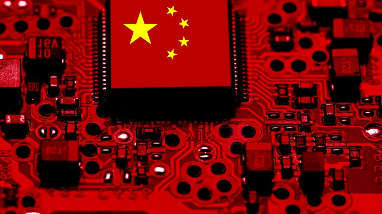
Washington thought it could freeze China's artificial intelligence ambitions by cutting off the supply of advanced Extreme Ultraviolet (EUV) lithography machines. They assumed that if you can't print sub-3-nanometer transistors on a flat piece of silicon, you can't build a world-class AI processor. They were wrong.
A high-profile Chinese AI chip startup called Shanghai Orient Computing Core Technology, led by semiconductor veteran Shaojun Wei, recently exited stealth mode with a massive valuation of 12.2 billion yuan (about 1.8 billion dollars). Wei isn't just another tech entrepreneur. He's the vice-president of the China Semiconductor Industry Association and a respected professor at Tsinghua University. His new venture isn't trying to out-print TSMC or ASML. Instead, Orient Computing is betting everything on 3D stacking and chiplet architectures to bypass US export controls entirely.
This isn't an isolated experiment. It's part of a massive structural pivot across China's entire tech ecosystem, spearheaded by giants like Huawei and fueled by cutting-edge software engineering from companies like Zhipu AI and DeepSeek. China is proving that you don't need the world's smallest transistors if you know how to stack and connect the ones you already have.
The Silicon Workaround Nobody Saw Coming
For decades, the semiconductor industry followed a predictable path: draw smaller lines, cram more transistors onto a flat plane, and watch performance rise. But flat silicon has hit a physical wall, and for China, a geopolitical one. US sanctions legally prevent Chinese foundries from purchasing the machinery required to produce top-tier, single-die GPUs that compete directly with Nvidia's flagship hardware.
So, how do you match the processing power of an advanced monolithic chip without advanced printing equipment? You stack mature nodes vertically.
Think of it like urban planning. If a city runs out of land to build massive sprawling estates, it doesn't stop growing. It builds skyscrapers. By using advanced packaging techniques like hybrid bonding, engineers can stack multiple independent chiplets directly on top of each other.
This architectural shift exploits a loophole in the physics of computing. A 7-nanometer or even a mature 14-nanometer chip stacked in three dimensions can achieve data transfer speeds and processing densities that rival much smaller, flat transistors. It completely changes the economics and physics of hardware manufacturing.
The Math Behind Spatial Scaling
To understand why this works, you have to look at latency and bandwidth. In a traditional computer setup, data travels relatively long distances across a motherboard between the processor and the memory. This travel time creates a massive bottleneck for AI workloads, which require shifting trillions of parameters every second.
When you stack memory directly on top of the logic layer, the physical distance data must travel shrinks from millimeters to micrometers. Huawei's heavily discussed LogicFolding architecture and its new Tau ($\tau$) scaling theory focus precisely on this concept. Rather than focusing purely on transistor size, they optimize for signal propagation speed and vertical interconnect density.
When you reduce the distance data travels, you drastically cut down on power consumption and heat dissipation per calculation. It means China can use readily available, older fabrication equipment to build stacked processors that punch way above their weight class.
Why the Market Misjudged the Sanctions
Silicon Valley assumed that keeping Nvidia's top chips out of Beijing's hands would cause Chinese AI models to fall years behind. That assumption ignored the power of hardware-software co-design.
Look at what happened with the release of Zhipu AI’s GLM-5.2 model and recent updates from DeepSeek. These companies are building highly sophisticated, open-weight AI models that rival American counterparts like Anthropic's Claude or OpenAI's systems in specific tasks like automated vulnerability detection. They aren't doing this on massive arrays of Nvidia H100s. They're optimizing their algorithms to run natively on domestic clusters powered by stacked architectures.
When you control both the chip design and the software framework, you can bypass traditional hardware limitations. By tuning the AI model to accommodate the specific latency profiles of a 3D-stacked chip, Chinese developers are squeezing maximum efficiency out of domestic hardware like Huawei's Ascend series and Orient Computing's modular chiplets.
The Real Engineering Hurdles
It's not all smooth sailing, though. Stacking chips vertically introduces two massive engineering headaches that the industry is aggressively trying to solve:
- Thermal Management: When you stack high-performance processors on top of each other, heat gets trapped in the middle layers. If you can't cool the center of the chip stack, the silicon will throttle or melt.
- Yield Rates: Connecting multiple layers requires drilling thousands of microscopic holes called Through-Silicon Vias (TSVs). If even a few of these vertical connections fail during manufacturing, the entire expensive stack becomes scrap metal.
These are the exact issues that advanced packaging research teams are tackling right now. The race isn't about who can buy the next ASML lithography machine anymore. The real race is about who can master hybrid bonding and thermal dissipation in multi-layered silicon structures.
What Happens Next
If startups like Orient Computing and established tech giants scale these 3D architectures successfully, the global semiconductor market will split into two distinct ecosystems. One will rely on hyper-advanced, incredibly expensive sub-2-nanometer flat printing. The other will rely on highly complex, sovereign 3D packaging environments built on mature nodes.
If you're building infrastructure or investing in AI technology, you need to stop measuring a nation's computing power solely by the nanometer metrics of its foundries. The metric that actually matters moving forward is vertical interconnect density.
Keep an eye on the development of open-source software stacks designed to replace Nvidia's proprietary CUDA framework. The true test of China's hardware pivot won't just be how high they can stack their silicon, but how effectively their software can unite thousands of these modular, vertical processors into cohesive, massive datacenters.